The controllable preparation of high-quality two-dimensional atomic crystals is a prerequisite for basic research and application development. At present, it is one of the major basic scientific issues that urgently requires prior research. The ultimate goal of controlled preparation is to obtain two-dimensional atomic crystals of large area, single layer and single crystal structure.
With the strong support of the Chinese Academy of Sciences, the Ministry of Science and Technology, and the National Natural Science Foundation of China, researchers from the Organic Solids Laboratory at the Institute of Chemistry, Chinese Academy of Sciences have made important progress in the controlled preparation and performance of graphene and boron nitride. The results were published on Adv. Mater.
Single crystal graphene is grown directly on the dielectric layer. Chemical vapor deposition (CVD) has become one of the most important methods for the preparation of graphene because it combines the advantages of high quality and macro quantities. However, graphene prepared by this method generally needs to be transferred to other dielectric layers to prepare graphene devices and circuits. The transfer process will cause problems such as graphene damage, wrinkles, contamination, and material waste.
Therefore, whether the graphene can be directly grown on the dielectric layer has important scientific significance and huge technical requirements. It is compatible with the current silicon electronics processing process, graphene does not need to transfer, can be directly used for device preparation and assembly. In previous work, the researchers invented the oxygen-assisted method to prepare graphene films directly on silica insulation (J. Am. Chem. Soc. 2011, 133, 17548). Later, they also found that by controlling the size of the nucleation sites and crystallographic regions of graphene by two chemical vapor deposition methods, direct growth on the silicon nitride surface was achieved. The size of graphene domain crystals in the prepared graphene film is up to 1 μm, and the mobility can reach 1510 cm2 V-1s-1 in air (Adv. Mater., 2013, 25, 992).
However, the graphene films prepared by the above two methods all have a polycrystalline structure. In this work, they developed a small gas flow, long time, and deposition methods under near-equilibrium conditions, and achieved non-metallic catalytic growth and controlled preparation of micro-scale graphene single crystals on a variety of insulating substrates. The largest graphene single crystal size is 11 μm (Fig. 1 left), which is 30 times as large as the graphene single crystal grown on the boron nitride substrate reported in the literature. This graphene single crystal has a perfect crystal structure, and the surface is clean, wrinkle-free, and undamaged. The field effect transistor made from it has a mobility of more than 5000 cm2 V-1s-1.
The study successfully implemented the Chinese saying “going slowly and working fineâ€, that is, under conditions of small airflow and close to equilibrium, the carbon atoms decomposed by methane have enough time to self-assemble into single crystal graphene. The results of this study were published in "Advanced Materials" (Adv. Mater., 2014, 1348-1353) and were selected as the inner cover (Figure 1 right).
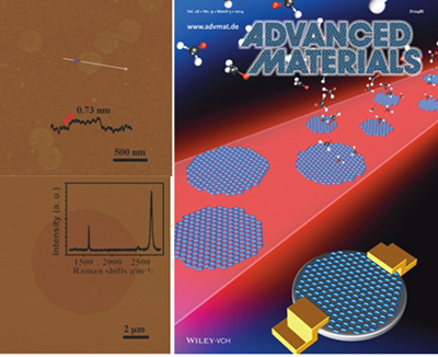
Figure 1 AFM Photograph of Single Crystal Graphene (left) and Inner Cover of Advanced Materials (right)
Preparation of hexagonal boron nitride (h-BN) monolayer films with large domain size. In recent years, the research of graphene in the field effect transistor has attracted people's attention. The field effect device is mainly assembled on the basis of silicon dioxide/silicon. The charge scattering and surface caused by the impurities on the surface of silicon dioxide. The presence of dangling bonds and charge traps thus fails to fully demonstrate the excellent properties of graphene itself.
Hexagonal boron nitride is a 2D layered structure of wide bandgap (5.9 eV) graphene. It has a lot of excellent properties, such as: high temperature stability, good mechanical properties, good thermal conductivity, and moderate dielectric properties. The constant (~4) makes it have a wide range of application prospects; at the same time, its surface has no impurity charge, dangling bonds and charge traps, and ultra-high degree of lattice matching with graphene (greater than 98%). These properties determine Its dielectric layer as a field effect device is significantly better than silicon dioxide.
At present, the preparation of h-BN is mainly performed by chemical vapor deposition (CVD). The main problem is that the size of the monolithic h-BN in the preparation process is small, thereby increasing the grain boundary of the film and reducing the quality of the film. At the same time, the presence of impurities at the graphene and h-BN interface also reduces its performance as a dielectric layer in graphene field effect devices.
In response to these problems, the relevant researchers of the Solid State Key Laboratory of Chemical Engineering collaborated with Prof. H. Hu of HIT to prepare a monolithic triangular h-BN with a size of 20 μm (top left in Figure 2) by CVD, and further grow to obtain a continuous film. This reduces the grain boundary of the film and improves the quality of the film. Due to the high stability and oxidation resistance of h-BN, the film transferred on the silica/silicon substrate assisted by polymethyl methacrylate was heat-treated in air to remove residue from the transfer process, resulting in a surface Clean h-BN film. The field-effect device (Fig. 2 bottom left) assembled from it into graphene showed a 6-fold increase in mobility compared to the device without heat treatment. The research results were published in "Advanced Materials" (Adv. Mater., 2014, 26, 1559-1564) and were selected as the inside cover (Figure 2 right).
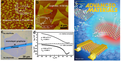
Figure 2 AFM image of triangular boron nitride (upper left); field-effect device and transfer curve prepared from boron nitride, graphene (bottom left); inside cover of Advanced Materials (right)
Brass fasteners are used for their physical and aesthetic properties. Brass is utilized due to its high thermal conductivity and corrosion resistant properties, it is suitable for use in hot and cold environments, and resistant to water corrosion, making it a staple of industries such as heating and plumbing. Brass fasteners are largely non-magnetic (like any fastener, slight magnetic properties can develop during the manufacturing process) and resistant to tarnishing.
Brass fasteners are suited for some marine environments, including brackish water and slow current sea water; brass in this environment develops a protective green coating. Brass fasteners are also commonly used with wood applications, as the golden coloring blends well with the tan wood. Brass is a softer metal and must be used with care, always drilling pilot holes and using driver bits that fit the head of the screw precisely to prevent stripping. Brass Bolts also require a pilot hole be driven before installtion.
Brass Nut,Adjustable Brass Nut,Brass Strat Nut,Brass Cap Nut
Taizhou Hongchuang Hardware Co., Ltd. , https://www.jstaizhouhongchuang.com